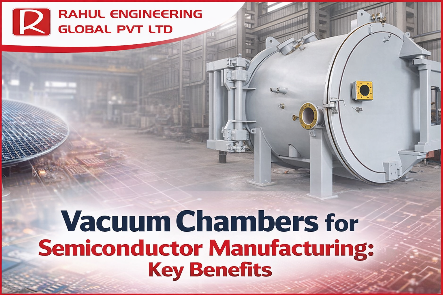
Importance of Vacuum Chambers in Semiconductor Manufacturing
Semiconductor fabrication involves advanced processes such as deposition, etching, ion implantation, and thin-film coating. Many of these processes require a clean, controlled environment to ensure accurate results.
Vacuum chambers provide several advantages in semiconductor production, including:
- Elimination of air contaminants
- Controlled processing environment
- High precision manufacturing
- Improved product reliability
- Consistent process quality
Because semiconductor devices are extremely small and complex, maintaining a contamination-free environment is critical.
Key Benefits of Vacuum Chambers for Semiconductor Manufacturing
1. Contamination-Free Processing
One of the primary benefits of vacuum chambers is the ability to remove air particles, dust, and moisture that could damage semiconductor wafers.
Semiconductor manufacturing requires ultra-clean environments to avoid defects. Vacuum chambers help maintain these conditions by preventing contamination during critical production steps.
2. High Precision Thin-Film Deposition
Many semiconductor components require thin layers of materials to be deposited on silicon wafers. These thin films must be applied with extreme accuracy.
Vacuum chambers support advanced deposition techniques such as:
- Physical Vapor Deposition (PVD)
- Chemical Vapor Deposition (CVD)
- Atomic Layer Deposition (ALD)
These processes require vacuum conditions to achieve uniform and precise material coatings.
3. Improved Process Control
Vacuum chambers allow manufacturers to precisely control pressure, temperature, and gas composition during semiconductor fabrication.
This level of control ensures consistent production results and improves manufacturing efficiency.
4. Enhanced Product Quality
Defects in semiconductor devices can lead to performance issues or product failure. Vacuum chambers reduce contamination and environmental interference, ensuring higher product quality and reliability.
This is particularly important for industries such as electronics, telecommunications, and computing.
5. Support for Advanced Semiconductor Technologies
Modern semiconductor devices, including microprocessors and memory chips, require advanced fabrication techniques. Vacuum chambers support critical processes such as plasma etching, wafer coating, and surface modification.
These technologies are essential for producing next-generation electronic devices.
6. Energy Efficiency and Process Optimization
Vacuum chamber systems help optimize semiconductor manufacturing processes by reducing unnecessary material loss and improving production efficiency.
Efficient vacuum environments also help reduce energy consumption during fabrication processes.
Materials Used in Semiconductor Vacuum Chambers
Vacuum chambers used in semiconductor production are typically constructed from materials that provide strength, corrosion resistance, and minimal contamination risk.
Common materials include:
- Stainless steel
- Aluminium alloys
- Titanium components
- Special vacuum-compatible coatings
These materials help maintain stable vacuum conditions and long equipment lifespan.
Applications in Semiconductor Manufacturing
Vacuum chambers are used in several semiconductor production processes, including:
- Wafer Processing: Vacuum chambers enable controlled environments for silicon wafer processing and treatment.
- Thin-Film Deposition: Used to apply thin material layers on semiconductor wafers for circuit formation.
- Plasma Etching:Vacuum environments support plasma-based etching processes used to create microscopic circuit patterns.
- Surface Analysis and Testing:Vacuum chambers help analyze semiconductor materials without contamination.
Choosing the Right Vacuum Chamber for Semiconductor Manufacturing
Selecting the right vacuum chamber is essential for ensuring optimal performance and efficiency. Manufacturers should consider several factors:
- Chamber size and capacity
- Material compatibility
- Pressure range capability
- Integration with semiconductor processing systems
- Maintenance and cleaning requirements
Working with experienced vacuum chamber manufacturers helps ensure the equipment meets specific semiconductor production needs.
Conclusion
Vacuum chambers play a critical role in semiconductor manufacturing by providing a controlled and contamination-free environment for advanced fabrication processes. From thin-film deposition to plasma etching, these chambers support the precise conditions required to produce modern electronic devices.
By improving process control, reducing contamination, and enhancing product quality, vacuum chambers help semiconductor manufacturers maintain high production standards and technological innovation.